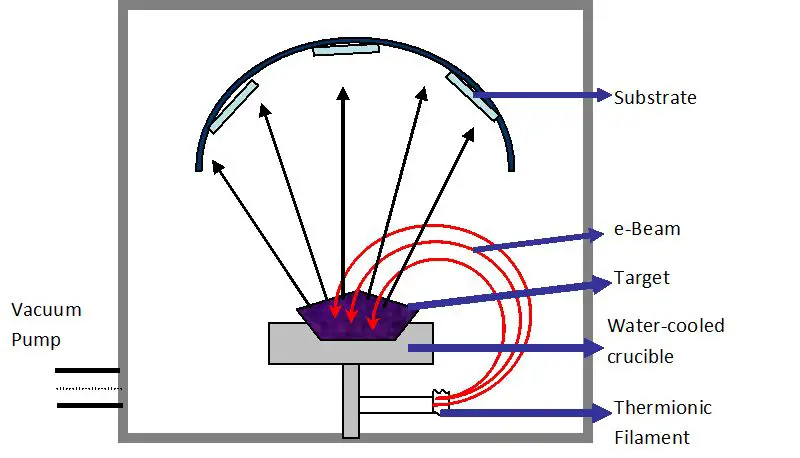
Electron beam evaporation
Electron beam evaporation, also known as E-beam evaporation, occurs when a target material is blasted with an electron beam that is given off by a tungsten filament under a high vacuum. Electron beam evaporation is used at ZC&R Coatings for Optics and Abrisa Technologies. This process is not the most commonly used procedure, but it does have several uses and there are several little known facts about E-beam evaporation.
Electron Beam Evaporation Facts
Here are 8 electron evaporation facts listed below:
- The deposition rate in electron beam evaporation can be as low as 1 nanometer per minute and as high as 2 micrometers per minute.
- It is wear resistant and has thermal barrier coatings, making it ideal for aerospace industries.
- The hard coatings are ideal for cutting and tool industries.
- The electronic and optical films created in the E-beam evaporation process are great for thin film solar applications and within the semiconductor industries.
- Electron beam evaporation is a line of sight deposition process and when performed at a low pressure.
- The inner surface of complex geometries cannot be coated, only the outer surface because of the translational and rotational motion of the shaft.
- Non-uniform evaporation rate can occur due to the filament degradation within the electron gun.
- Scattering of the vapor cloud takes place when vapor deposition is performed a higher pressure. This means that the surfaces not in sight of the source can be coated.